
Material science: Nils Hauff, nils.hauff@umu.se
VolumeEM: Sara Henriksson, sara.henriksson@umu.se
Cryo-EM:
FIB-SEMs are used in both material science and life science and can operate at both room temperature and cryo conditions. FIB-SEM microscopes belong to the family of SEM but are equipped with two beams:
• Electron beam, non-destructive, for imaging
• Ion beam, destructive, for sample modification
When the sample is perfectly arranged with the two beams, coming at different angles towards the sample, they will reach and image the same area. Both beams can be controlled independently. While the electron beam is used for non-destructive imaging, as in a conventional SEM, the ion beam does actively modify the sample. Upon impact on the sample, the ion-beam will mill into the sample both due to the ion’s higher mass and because ions deposit all their energy into a much smaller volume. By intentionally only scanning selected areas with the ion-beam, we can therefore selectively remove small volumes of material in a controlled way.

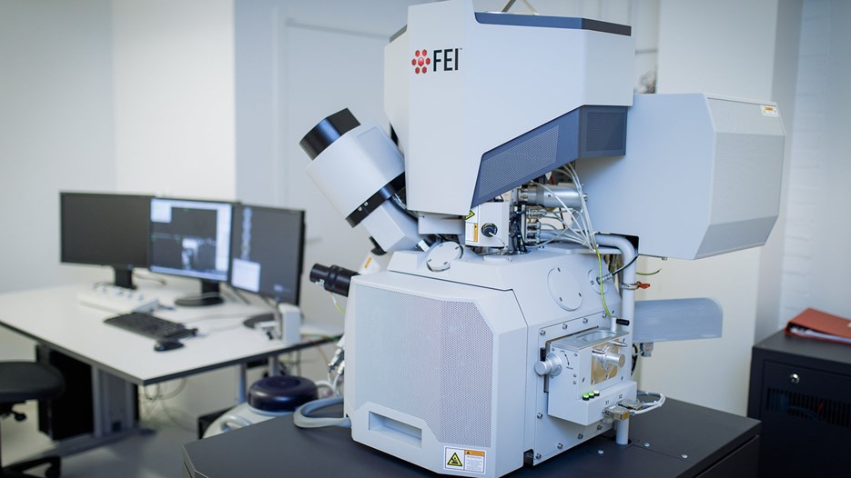
Overview of a FIB-SEM setup
Image UCEMSince the ion beam and the electron beam come at an angle, while coinciding in a chosen area on a sample, both imaging and milling can be done simultaneously. The most basic application is to mill a clean cross section with the ion beam and image the cross section with the electron beam. To only mill certain areas but protect others, FIB-SEMs are typically equipped with a Gas Injection System (GIS). A GIS can be utilised to cover selected areas with a protective coating, enabling cleaner cross sections.
More advanced applications of FIB-SEM are the fabrication of TEM lamellas, lift-out of volumes (typically onto TEM grids) using a lift-out needle, and volume imaging. Any detector can be used or acquired consecutively during the milling process to generate a 3D-reconstruction of your sample.
Material science
In material science, FIB-SEM excels at preparing cross-sections of materials—especially where features of interest are buried deep within the bulk—to expose internal microstructures for basic inspection, alongside high-resolution SEM imaging for morphology analysis and EDS mapping for elemental composition. It also enables site-specific sample preparation—including lift-out techniques—for advanced methods like TEM lamella thinning to probe nanoscale structures, TEM tomography for 3D structural reconstructions, and STXM for chemical analysis of organics. Volume imaging through slice-and-view tomography produces detailed 3D reconstructions of pore networks in shales, alloy microstructures, or composite materials, offering superior correlative imaging over standalone SEM. Unlike traditional polishing or broad-beam milling methods, FIB-SEM provides nanometer-precision targeting and in-situ imaging, making it indispensable for revealing subsurface details inaccessible to surface-only techniques.
Contact person: Nils Hauff, Nils.Hauff@umu.se

Gold pillars with Nickel core.
Image Nils HauffVolumeEM
Focused Ion Beam Scanning Electron Microscopy (FIB-SEM) is used for volume imaging to answers scientific questions about the 3D context of cells, cell-cell contacts or organelles in tissue. The sensitive in-lens backscattered electron detector will reveal compositional differences in the sample. For biological samples, this means that we are able to see membranes, larger protein complexes, etc., similar to a conventional TEM. The ion beam mills the surface of the sample perpendicular to the electron beam, and the sensitive in-lens backscattered electron detector can then image the freshly exposed surface. Cycles of repetitive milling and scanning result in a 3D image volume of the sample, with equal resolution (5-20 nm) in all (x, y and z) dimensions. After computational alignment of a stack of images into a 3D-volume, cells and organelles can be segmented and provide a visual 3D model of the selected cell or tissue volume. FIB-SEM is site-specific; this function of selecting a particular volume is very useful for correlated light and electron microscopy (CLEM), when a small volume is localised and of particular interest.
Contact person: Sara Henriksson, sara.henriksson@umu.se

FIB-SEM volume of a SARC-CoV-19 infected cell, revealing cellular context and dynamic interactions between organelles. Video: Sara Henriksson.

Segmented mitochondria from mechanically dissected muscle tissue. Gineste, C. et.al., Enzymatically dissociated muscle fibers display rapid dedifferentiation and impaired mitochondrial calcium control. iScience, 25(12). https://doi.org/10.1016/j.isci.2022.105654
Cryo-EM
Cryo FIB-SEMs are equipped with a stage that is cooled down with liquid nitrogen for samples that need to be kept frozen, e.g. plunge frozen cells. Cryo FIB-SEM is often used to thin down samples that are too thick to be directly imaged by cryo-electron tomography. For such samples, the ion beam is mainly used for preparing thin lamellas, like a window, inside the sample. This lamella is thin enough to later be imaged with a TEM: tilt-series acquisition can be acquired and after data-processing, tomograms can be reconstructed to visualise the 3D-volume of the sample. The lamellae can either be kept attached to the sample on the grid or moved to another TEM-grid with a lift-out needle.
The facility is also equipped with a micro patterning device (Primo) to assist in positioning the cell to the center of the grid square.
We also have a fluorescence light microscope that operates at cryo-conditions (Leica cryo thunder), which will help to target the areas of interest.
Contact persons:
Lorene Gonnin, lorene.gonnin@umu.se
Erin Schexnaydre, erin.schexnaydre@umu.se

Sample preparation for Cryo-lamella. Wagner, F.R. et.al., Preparing samples from whole cells using focused-ion-beam milling for cryo-electron tomography. Nat Protoc 15, 2041–2070 (2020).
The Thermo Scientific™ Scios™ DualBeam™
More details
UCEM facility in the KBC building - Map to UCEM can be found at this link
- Accelerating voltage: 200 V - 30 kV (EB); 500 V - 30 kV (IB)
- Electron emitter: Thermal field emission
- Ion emitter: Ga LMIS
- Detector: Trinity T1/T2, ET-SE, ICE, DBS, CCD, Nav-Cam
- Stage configuration: 5-axes eucentric motorized
- System control: xT GUI with additional options (GIS, ASV, AutoFIB, AutoTEM)
- System mode: High-vacuum @ RT
- Electron Optics with 1.4 nm resolution at 1 kV and 1 pA – 400 nA beam current range
- Ion Optics with 3.0nm resolution at 30 kV and 1.5 pA – 65 nA beam current range
- ELPHY Plus electron beam lithography system (20 MHz pattering frequency, 1 ns dwell time increment)
The Thermo Scientific™ Aquilos 2 Cryo-FIB

More details
The UCEM facility in the KBC building, you can find it on this link.
- Accelerating voltage: 200 V - 30 kV (EB); 500 V - 30 kV (IB)
- Electron emitter: Thermal field emission
- Ion emitter: Ga LMIS
- Resolution Electron Optics: 1.6 nm at 30 kV, 2.6 nm at 2 kV (at room temperature), 6.0 nm* at 2kV (at cryo-temperature)
- Resolution Ion Optics 7.0 nm* at 30 kV
- Detector: Trinity T1/T2, ET-SE, CCD, Nav-Cam
- Stage configuration: 5-axes eucentric motorized
- System control: xT GUI with additional options (GIS, Micromanipulator for TEM lamellas, Plasma coater, ASV, AutoFIB, AutoTEM)
- System mode: High-vacuum @ RT or cryogenic temperature
Material science: Nils Hauff, nils.hauff@umu.se
VolumeEM: Sara Henriksson, sara.henriksson@umu.se
Cryo-EM: