NanoLab must be acknowledged in any kind of articles (publications) when data/devices are produced with the equipment of the NanoLab. Bibliographic information must be sent to Roushdey Salh for archiving purposes.

Research infrastructure NanoLab is an open-access infrastructure, providing facilities in nano materials characterization located at the Department of Physics.
We are an open-access infrastructure located at the Department of Physics, which means anyone can use our equipment after having an adequate training. NanoLab provides the possibility to:
Besides, NanoLab is a classified cleanroom (ISO 5) that can be used for your own experiments.
The Nanolab was established in June 2012, and has since its inception been in continuous development. Today, it comprises a variety of advanced fabrication and characterization setups, including a mask aligner (Karl Süss Mask Aligner MJB3), a nanoimprinter (Obducat NIL 2.5), a thin-film deposition system (PVD75 thermal evaporator), X-ray diffractometer (PANalytical Xpert3 Powder), a contact angle meter, and a spin coater, as well as number of more standard pieces of equipment, such as vacuum ovens, hotplates, optical microscopes, UV-curing boxes, and analytical scales. A short overview of the available equipment can be found below:
As NanoLab's environment is extremely clean (approximately 100,000 to 300,000 times cleaner than a regular room in terms of airborne particles), it is possible to manufacture and study materials with notably high standard and precision. The facility is currently an invaluable tool for the University´s rapidly expanding research in the fields of microelectronics, optics and photonics, and nanotechnology, but it is also of obvious interest for scientists that are interested in, e.g., the fabrication and/or appropriate characterization of thin films, or materials that feature structures on the micrometer or sub-micrometer level. As such, its potential users encompass experimental researcher in essentially a wide variety of fields in natural science and medicine.
Director of the NanoLab (Dr.rer.nat. Roushdey Salh), Department of Physics.
The equipment in NanoLab is made available to all scientists at Umeå University, as well as external institutions, for a fee of 300 SEK per hour for major users (>50 hours). It is possible for high-volume users to apply for a discount. The NanoLab manager offers training sessions on each piece of equipment on an annual basis or on demand, and after approval following the training the user can independently use the equipment he or she has been trained on. Non-approved users can only use a piece of equipment under the supervision of the manager. Manuals and handbooks have been developed for each piece of equipment, and are available online or beside the equipment.
All of the equipment in NanoLab is available for booking during normal work days, and the booking system is available at:
www.phys.umu.se/cleanroombooking
Training and special courses concerning the equipment are offered annually often in November or December (exact date announced under KBC research courses), but also possible on demand.
NanoLab is used for both undergraduate education (grundutbildning) and graduate teaching. Two advanced courses on the undergraduate level (Nano Science 7.5hp and Advanced Materials 7.5hp) currently use NanoLab as their laboratory facility in which the experiments are carried out. Three courses on the graduate level (Cleanroom technology 1.5 ECTS, Physical thin film deposition 1.5 ECTS, and Atomic Force Microscopy 1.5 ECTS) are also offered annually and are announced at the KBC website. These courses have primarily attracted participants from the Physics, Chemistry and Applied Physics departments, but participants from the international business program and the department of Clinical Microbiology have also attended. Specific teaching and training sessions have also been offered on a regular basis to interested users. The courses are given in English, and the numbers of students are between 20 and 40 in each undergraduate course, and between 10 and 20 in each graduate course. For the coming years, courses are planned in Nano-imprinting and Material surface modification.
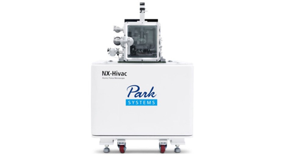
Park NX-Hivac enables material research that requires high accuracy and high resolution measurements in a vacuum environment. High vacuum measurement offers greater accuracy, better repeatability, and less tip and sample damage than ambient or dry N2 conditions.
Specification:
Vacuum level: E10-5 torr
Vacuum chamber: 300 mm x 420 mm x 320 mm
XYZ scanner: X-Y 100 μm x 100 μm and Z 15 μm
Optics: 10× Objective lens, 5M pixel CCD
Sample stage size: 50 mm x 50 mm
Sample size: up to 150 mm x 150 mm
Sample thickness: up to 20 mm
Park NX-Hivac/ High vacuum AFM: https://youtu.be/z6Wle8Uq4oQ
Park SmartScan/Operating Software: https://youtu.be/3jzHUaOlr5U
Park SmartAnalysis/Analysis Software: https://youtu.be/BD-aAHyd5TI
Applications:
1. Surface imaging and topography by:
Contact Mode https://youtu.be/4bgb5nD2JOU
Non-Contact Mode https://youtu.be/J3YB_hemZ4w
Tapping Mode https://youtu.be/En1S-HX4o-M
PinPoint Mode https://youtu.be/z5F8-18of_I
Force modulation mode https://youtu.be/QcJTrha8atM
2. Nanomechanical properties
Force Modulation Microscopy (FMM) https://youtu.be/QcJTrha8atM
Lateral Force Microscopy (LFM) https://youtu.be/UKK9XoeeWBA
Nanoindentation https://youtu.be/CKHit_kzFE0
Force Distance Spectroscopy https://youtu.be/KKYPj3FUW5k
Force Volume imaging
3. Electrical properties
Conductive Probe AFM (CAFM) https://youtu.be/46_2QjqEq6w
Electrostatic Force Microscopy (EFM) https://youtu.be/7UVSD2e2rjE
Kelvin Probe Force Microscopy (SKPM) https://youtu.be/PTrIiKE8peI
Dynamic Contact EFM (DC-EFM) https://youtu.be/hAe9nwOX_eg
Piezoelectric Force Microscopy (PFM) https://youtu.be/jqpS41y4jCE
4. Nanolithography https://youtu.be/6J_v-C7Dozw
Achieved mechanically deforming the sample surface (scratch the sample surface with hard tips), or by changing of the surface's chemical properties (apply a bias between the tip and the surface). Objects can be drawn (bitmap images) in the software and printed onto the sample surface.
5. Optional features (not included in our system)
I-V Spectroscopy https://youtu.be/gLy7ro6-xEY
Tip Enhanced Raman Spectroscopy https://youtu.be/6aH2J6NSTsE
Scanning Capacitance Microscopy https://youtu.be/OfMS9Xjv4vY
Scanning Thermal Microscopy https://youtu.be/55RAIa0oYg0
Magnetic Force Microscopy https://youtu.be/1xLNoMMy-rM
Scanning Ion Conductance Micros https://youtu.be/ps0w0Dm47ag
Near Field Scanning Optical Micros https://youtu.be/FNaHhaz9MGo
User manual: Atomic force microscope (Park NX-Hivac)
Official manual: AFM Park NX-Hivac
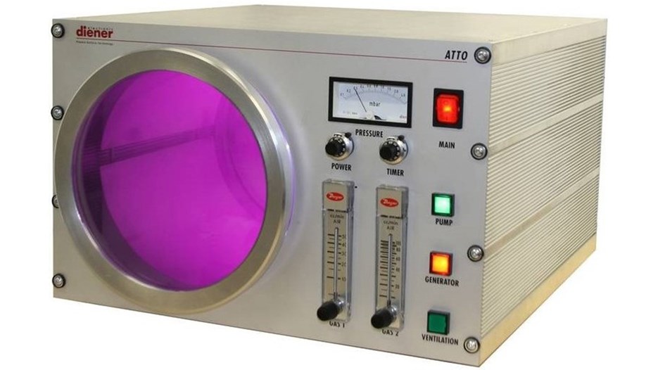
is used for varieties of surface treatment, such as: cleaning, surface activation, etching. Samples can be up to 20 cm in diameter, two inlet gases are available (usually argon and oxygen).
User manual: Plasma cleaning system ATTO
Official manual: Atto Deiner Plasma Cleaner
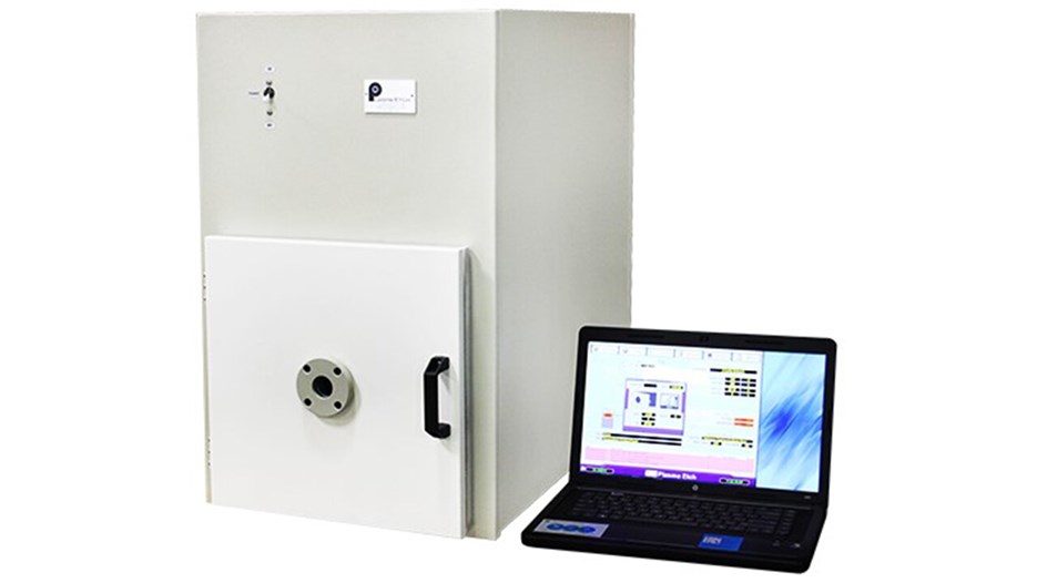
The PE-100 is a complete plasma treatment solution capable of plasma functionalization, etching of semiconductor, hydrophilic surface modification, surface cleaning, surface preparation, removal of Hydrocarbons and more. Five inlet gases are available, mixing gases and running are fully recipe controlled, 300 Watt Generator at 13.56 MHz.
User manual: Plasma cleaning/etching system PE-100
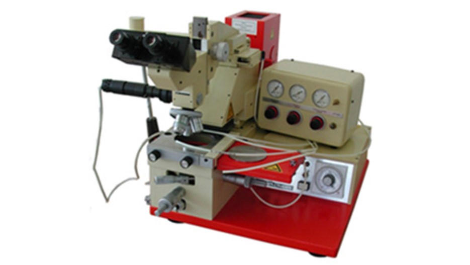
is used for UV photo lithography using 350 W mercury lamp and Suss diffraction-reducing exposure optics. The primary exposure wavelengths of 365 or 403 nm lead to about 5 μm minimum resolution.
User manual: Karl Süss Mask Aligner MJB3
Official manual: Karl Süss Mask Aligner MJB3
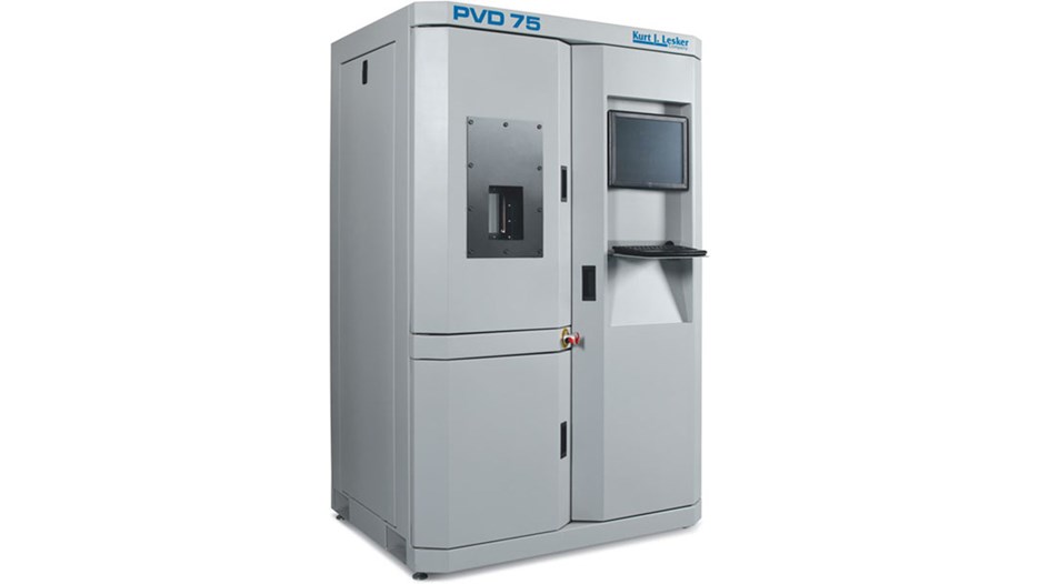
is used for producing metallic or organic thin layers between 1-400 nm at high vacuum pressure 5x10⁻⁸ Torr. The system has 3 normal deposition sources and 1 low temperature organic deposition source. Samples can be up to 30 cm in diameter, substrate rotation and heating up to 350°C and two gas inlets are available.
User manual: Kurt J. Lesker PVD75 Thermal Evaporator
Official manual: Kurt J. Lesker PVD75 Thermal Evaporator
Kurt J. Lesker PVD75 Deposition Data
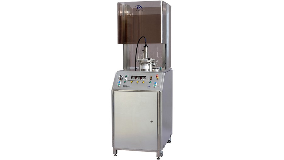
is used to stamp a pattern into a polymer coating on a substrate at max heating 250ºC and max pressure 70 bar. A stamp made of nickel or silicon. The substrate is heated and the stamp is pressed into the polymer. The resolution is up to 1 nm depending on the stamp.
User manual: Obducat NIL 2.5 Nanoimprinter
Official manual: Obducat NIL 2.5 Nanoimprinter
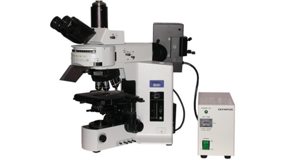
provides high contrast, high magnification, optimal color fidelity, Imaging in different modes and with different magnifications.
Official manual: Olympus BX51 Optical Microscope
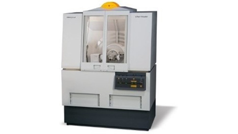
X-ray source : Cu Kα, λ=1.5418 Å.
Operating range: 10 - 70 o2θ,
small-angle X-ray scattering possible too.
Temperature: Room temperature, but a temperature chamber is available for lower and higher temperatures.
Humidity: Ambient, but a humidity chamber is available for different humidities.
Sample amount: App. 10 mg
User manual: PANalytical Xpert3 Powder XRD
Official manual: PANalytical Xpert3 Powder XRD
is used for producing thin layers from dissolved materials (liquids) at room temperature. Layer thicknesses (nm-μm range) controlled by the rotation speed between 1-10000 rpm.
Official manual: SPIN150-NPP Spin Coater
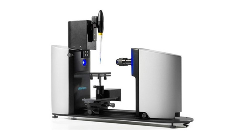
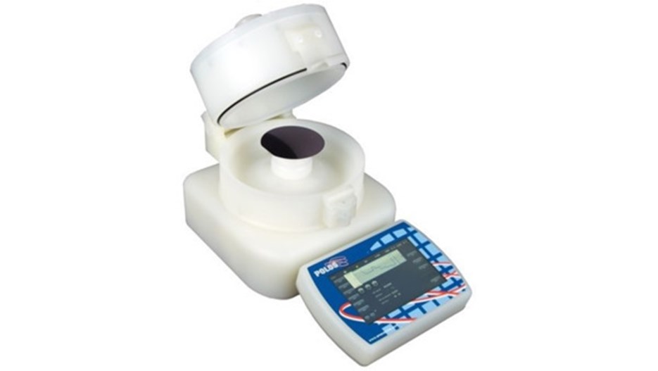
is used for highly accurate measurements of static and dynamic contact angle, measure surface free energy, surface and interfacial tension.
User manual: Theta OneAttension Contact Angle Meter
Official manual: Theta OneAttension Contact Angle Meter
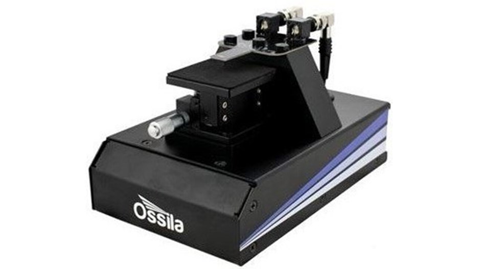
It is used to characterize thin layers electrical property of conducting and semiconducting materials. It is capable of delivering currents between 10 nA and 150 mA, and can measure voltages from as low as 100 μV up to 10 V. The system can measure sheet resistances in the range of 100 mΩ/square to 10 MΩ/square, enabling the characterization of a wide range of materials. If the sample thickness was provided, then the average resistivity and conductivity will also be displayed.
User manual: Four-Point Probe system
Official manual: Four-Point Probe system
Vacuum Chamber Furnace - VBF-1200X-H8
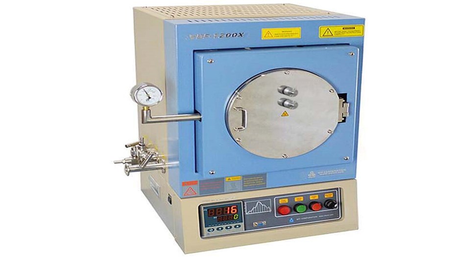
Designed for calcining or annealing semiconductor wafers (up to 6") under vacuum or various other gas atmospheres with a temperature of up to 1100°C. It equips a chamber made of a quartz tube sitting horizontally, with dimension 19 cm ID x 30 cm depth.
Working Temperature <= 1000 °C continuously, <= 1150 °C continuously is possible by using GE214 grade quartz tube, recommended heating rate 10°C/ min, Max. heating rate 20°C/ min, temperature uniformity: +/- 2°C. 30 segments program with ramping, cooling, and dwelling steps.
The furnace can achieve vacuum levels below 10-2 torr via mechanical pump within 30 minutes without thermal Block, 10-4 torr via turbo-pump within 30 minutes with the quartz thermal block at 900°C (available at the lab).
User manual: Vacuum Chamber Furnace - VBF-1200X-H8
Official manual: Vacuum Chamber Furnace - VBF-1200X-H8
Filmetrics F10-RT-UVX
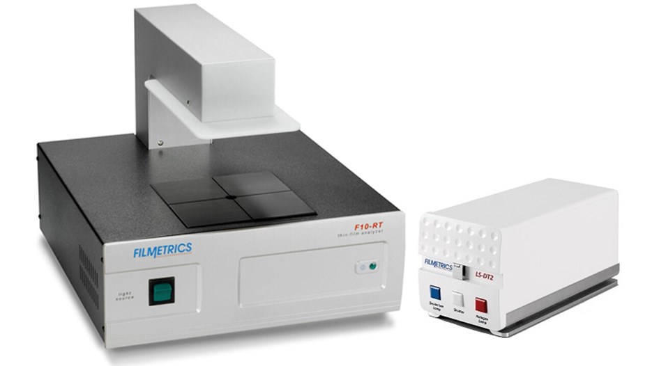
Thin film measurements system based on spectral reflectance (SR), is a non-contact technique that requires no sample preparation to measure film thickness. Light that is reflected from the film is analyzed in about one second to determine both a film’s thickness and refractive index. Multiple-layer films can also be measured.
Suitable mostly for transparent films, enabling measurements of films 30 Å to 100 μm thick films. The Filmetrics system Model F10-RT-UVX measures even translucent thin films made from virtually all common materials (metals) up to 200 nm. Typical accuracy is within a few angstroms.
User manual: Filmetrics F10-RT-UVX
Official manual: Filmetrics F10-RT_UVX
FLS1000 Photoluminescence Spectrometer

Measuring Fluorescence, Phosphorescence, Absorption, and Reflection spectra, besides delayed (time decay) Fluorescence and Phosphorescence at room temperature and at low temperature (liquid nitrogen temperature).
Solid (thin layer), liquid and powder sample holder are available
SENTECH SENresearch 4.0 Spectroscopic Ellipsometer

SENresearch 4.0 is a high-precision optical instrument used for non-destructive, sub-nanometer thin-film characterization, measuring thickness, optical constants (n, k), and material composition (from deep UV190 nm to NIR 3500 nm).
It provides the broadest spectral range with the best S/N ratio and the highest, selectable spectral resolution. High spectral resolution is offered to analyze even thick transparent films up to 200 µm thickness using FTIR ellipsometry. The measurement speed of FTIR ellipsometry compares to diode array configurations, which are also selectable up to 1,700 nm.
ARL QUANT'X Benchtop EDXRF Analyzer

The ARL QUANT'X is a benchtop Energy-Dispersive X-ray Fluorescence (EDXRF) spectrometer used for non-destructive elemental analysis. It is quickly detecting and quantifying trace elements from Fluorine (F) to Americium (Am) in almost any sample type (powders, thin films, granules, pastes, and liquids) without requiring known reference standards and also without requiring complex sample preparation. Operates in multiple atmospheres (air, helium, or vacuum) depending on the elements being targeted.
NanoLab must be acknowledged in any kind of articles (publications) when data/devices are produced with the equipment of the NanoLab. Bibliographic information must be sent to Roushdey Salh for archiving purposes.
Latest publications where NanoLab has been used